Cyclic Control Flow Graphs: Loop Unrolling
Posted on Sun 22 December 2024 in high_level_synthesis
Recall from Part III that we considered the GCD algorithm and manually converted this into RTL in FSMD form; we made no effort to automate this conversion. This was clearly a cop-out. In Part II we discussed an approach to scheduling which utilised the topological sort from a DFS, and were careful to curate those examples without any cycles; this is because the DFS only works on directed acyclic graphs (DAGs), i.e. those graphs which contain no cycles. Clearly this is a rather limiting constraint; the GCD had a backedge from while.body to while.cond, and consequently can't be scheduled using the DFS.
While I promise that we will get around to scheduling something like the GCD, for the moment it's convenient to treat a particular subset of algorithms which contain cycles; those algorithms with for-loops that can be unrolled.
Loop Unrolling
Loop-unrolling is an optimisation that compilers can undertake to manipulate loop nests. Consider a for-loop which iterates \(N\) times; this can be replaced with \(N\) duplicate statements, with the loop index variable substituted by the corresponding numerical value at each iteration. For instance, subjecting the following kernel
for (int idx=0; idx<N; ++idx) {
    c[idx] = a[idx] + b[idx];
}
to loop unrolling should yield something like the following:
c[0] = a[0] + b[0];
c[1] = a[1] + b[1];
c[2] = a[2] + b[2];
...
c[N-1] = a[N-1] + b[N-1];
For loop-unrolling in its simplest for, \(N\) should be a compile-time variable; this allows the compiler to unroll the loop nest fully (optimisations like loop-tiling can be undertaken on loop nests with runtime bounds, although we'll ignore this here for the sake of ease). The utility of this is clear for scheduling; we've completely eliminated the backedge resulting from the index bounds-checking and subsequent branching.
As an aside, you may be wondering why a compiler would want to provide this functionality in the first place. There are a few reasons, but principal amongst them are:
- Branching is an expensive operation for a CPU; it may require the flushing of an instruction pipeline.
- If there are no carried dependencies between loop iterations, SIMD operations can be leveraged (like in the vector addition example above).
An Example: Vector Addition
Consider the vector addition kernel:
#define SIZE 3
void vector_add(const int* __restrict__ a, const int* __restrict__ b, int* __restrict__ c) {
    for (int idx=0; idx<SIZE; ++idx) {
        c[idx] = a[idx] + b[idx];
    }
}
We can transform this into LLVM IR using the mem2reg and simplifycfg passes:
$> clang -O0 -Xclang -disable-O0-optnone -emit-llvm -S vector_add.c -o vector_add.ll
$> opt -S vector_add.ll -passes='mem2reg,simplifycfg' -o vector_add.ll
which yields:
define dso_local void @vector_add(i32* noalias noundef %a, i32* noalias noundef %b, i32* noalias noundef %c) #0 {
entry:
  br label %check

check:
  %loop_idx.current = phi i32 [ 0, %entry ], [ %loop_idx.next, %sum ]
  %done = icmp slt i32 %loop_idx.current, 3
  br i1 %done, label %sum, label %exit

sum:
  %a_idx = sext i32 %loop_idx.current to i64
  %a_ptr = getelementptr inbounds i32, i32* %a, i64 %a_idx
  %a_val = load i32, i32* %a_ptr, align 4
  %b_idx = sext i32 %loop_idx.current to i64
  %b_ptr = getelementptr inbounds i32, i32* %b, i64 %b_idx
  %b_val = load i32, i32* %b_ptr, align 4
  %c_val = add nsw i32 %a_val, %b_val
  %c_idx = sext i32 %loop_idx.current to i64
  %c_ptr = getelementptr inbounds i32, i32* %c, i64 %c_idx
  store i32 %c_val, i32* %c_ptr, align 4
  %loop_idx.next = add nsw i32 %loop_idx.current, 1
  br label %check, !llvm.loop !6

exit:
  ret void
}
where I've substituted the automated variable names for ones that are a little more descriptive. We can get LLVM to generate the CFG pictorially as follows:
$> opt -dot-cfg -disable-output -enable-new-pm=0 vector_add.ll

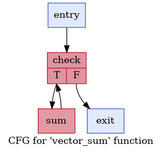
The mechanics of this are hopefully clear; we branch from the check basic block to the sum basic block, which subsequently branches back to check, and so on until check can finally branch to exit.
Loop Unrolling
We can enforce loop-unrolling through the addition of a further unroll-loops pass, where each loop iteration is implemented as a basic block which is branched to by the previous loop iteration's basic block:
define dso_local void @vector_add(i32* noalias noundef %a, i32* noalias noundef %b, i32* noalias noundef %c) #0 {
entry:
  ;; Compute c[0] = a[0] + b[0]
  %a_val = load i32, i32* %a, align 4
  %b_val = load i32, i32* %b, align 4
  %c_val = add nsw i32 %a_val, %b_val
  store i32 %c_val, i32* %c, align 4

  ;; Compute c[1] = a[1] + b[1]
  %a_ptr.1 = getelementptr inbounds i32, i32* %a, i64 1
  %a_val.1 = load i32, i32* %a_ptr.1, align 4
  %b_ptr.1 = getelementptr inbounds i32, i32* %b, i64 1
  %b_val.1 = load i32, i32* %b_ptr.1, align 4
  %c_val.1 = add nsw i32 %a_val.1, %b_val.1
  %c_ptr.1 = getelementptr inbounds i32, i32* %c, i64 1
  store i32 %c_val.1, i32* %c_ptr.1, align 4

  ;; Compute c[2] = a[2] + b[2]
  %a_ptr.2 = getelementptr inbounds i32, i32* %a, i64 2
  %a_val.2 = load i32, i32* %a_ptr.2, align 4
  %b_ptr.2 = getelementptr inbounds i32, i32* %b, i64 2
  %b_val.2 = load i32, i32* %b_ptr.2, align 4
  %c_val.2 = add nsw i32 %a_val.2, %b_val.2
  %c_ptr.2 = getelementptr inbounds i32, i32* %c, i64 2
  store i32 %c_val.2, i32* %c_ptr.2, align 4

  ;; Finished
  ret void
}
Clearly there are no loops here; the entire function has been implemented in a single basic block. Furthermore, since there are no carried loop dependencies, each element in the vector addition can be computed in parallel -- the first four instructions which deal with c[0] = a[0] + b[0] have no bearing on the subsequent sections where c[i] = a[i] + b[i] for \(i\gt 0\). This unrolling then allows us to extract concurrency from the loop nest; vector addition could, in principle, be implemented in an FPGA in \(\mathcal{O}(1)\) time, where the RTL resembles one large SIMD operation.
However, this does not come for free. For a start, unrolling the loop and simply doing a SIMD addition would require the RAM module to service the entire SIMD register in a single cycle, while our RAM module can only supply a single element per cycle. We could trivially alter the RAM module to provide burst access to the underlying memory, but this is a tweak we can defer to a later post. The more pressing issue is that we can't just arbitrarily unroll a loop since the FPGA has finite resources. We might be able to do this for a 100 or even 1000 element vector, but at some point we're going to run out of resources. Consider the case where we can only implement 10 ALUs in the FPGA fabric; then if the vectors have 16 elements, we can add 10 of the elements in a cycle, but the remaining 6 additions must be performed in a subsequent cycle. This problem is known as "binding", the mapping of operations to hardware resources. Hence, the schedule we obtain through analysis of the CFG only provides a "best case" schedule; we obtain a more realistic schedule when taking into account the constraints posed by binding.
List Scheduling
In the previous post, we alluded to some physical constraints of the RAM modules, in that only a single read or write can happen at a time, and that reads and writes cannot happen concurrently. For a realistic scheduling, these constraints must be provided for each resource that we use. An arithmetic unit that we use for addition, for instance, could take some non-zero number of cycles to produce a result; this is the latency of the resource. Similarly, we touched on the fact that there aren't infinite resources in the FPGA fabric allowing us to do an arbitrary number of additions in a single cycle. This combination of resource latency and number of a particular resource are the resource constraints, and must be accounted for when scheduling. This is referred to as list scheduling. List scheduling combines the heuristics we've talked about previously (ASAP and ALAP), but incorporates the physical resource constraints; if an instruction is ready to be scheduled by virtue of its dependencies having been resolved, there must be a physical resource with capacity to undertake the instruction, else it must be deferred to a later cycle where a resource is available.
For the vector addition example, we'll assume that we have a single adder resource which has a latency of three cycles. We'll find it convenient to have a dedicated adder entity which fakes the addition latency:
adder : process(clk) is
    variable count : integer := 0;
begin
    if rising_edge(clk) then
        if (rst = '1') then
            done <= '0';
            c    <= (others => '0');
        else
            if (start = '1') then
                count := 0;
            end if;
            count := count + 1;
            if (count = C_LATENCY) then
                c    <= std_logic_vector(unsigned(a) + unsigned(b));
                done <= '1';
            end if;
        end if;
    end if;
end process adder;
When the start signal is asserted for a single cycle, then the process shall do nothing for C_LATENCY cycles, and on the third subsequent clock rising edge shall return the values presented on the a and b ports, simultaneously asserting the done signal.
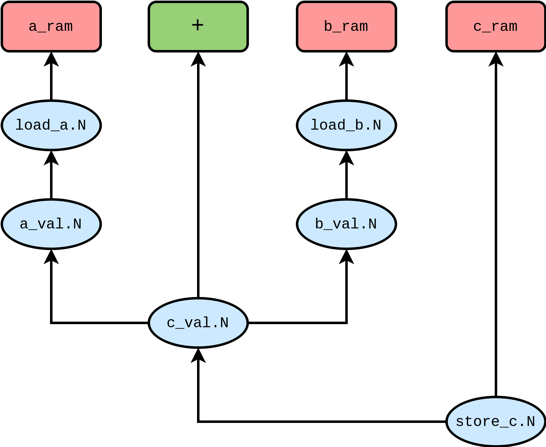
For the loop unrolled vector addition, we have the following dependency graph:

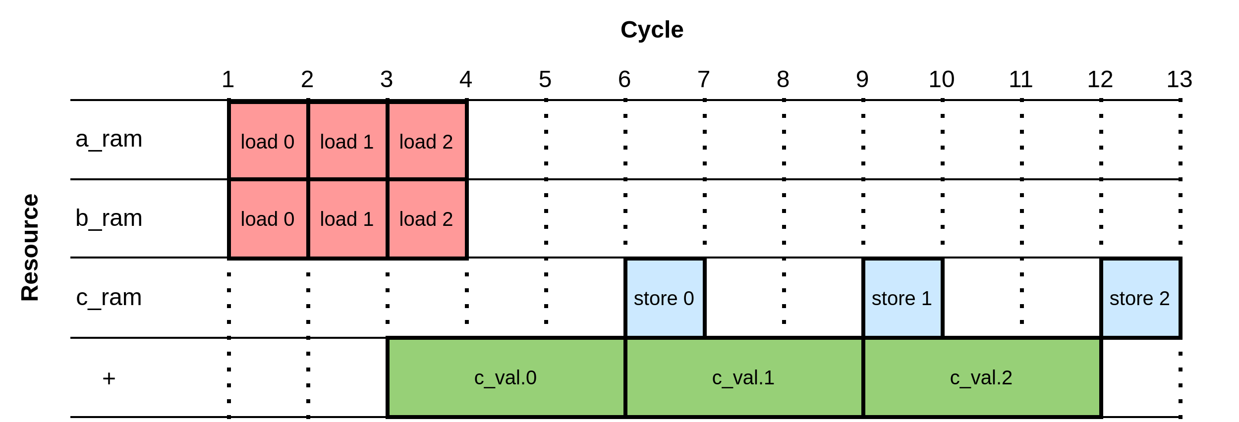
We can draw the corresponding schedule based on the resource utilisation at different times. The following depicts such a schedule; each resource is enumerated vertically, and each operation takes some number of clock cycles to complete, graphed as a horizontal span for a particular resource:

We see the effects of an ASAP schedule here; while load 1 and load 2 instructions aren't needed until cycles 6 and 9, respectively, to feed the adder resource, the a_ram and b_ram resources that they rely on are free from cycle 2. As a result, the instructions are scheduled as early as is practical. If we were to use the ALAP heuristic, then load 1 and load 2 would be scheduled on cycles 5 and 8, respectively, to feed the adder on the subsequent cycles.
You might wonder why there's a cycle delay between the end of load 0 and the start of the addition to compute c_val.0. The issue here is that once we've requested the values in the A and B RAMs, they must be registered so that they can persist on the input ports to the adder module, hence an additional cycle to register the values returned from the A and B RAMs is required.
FSMD Implementation
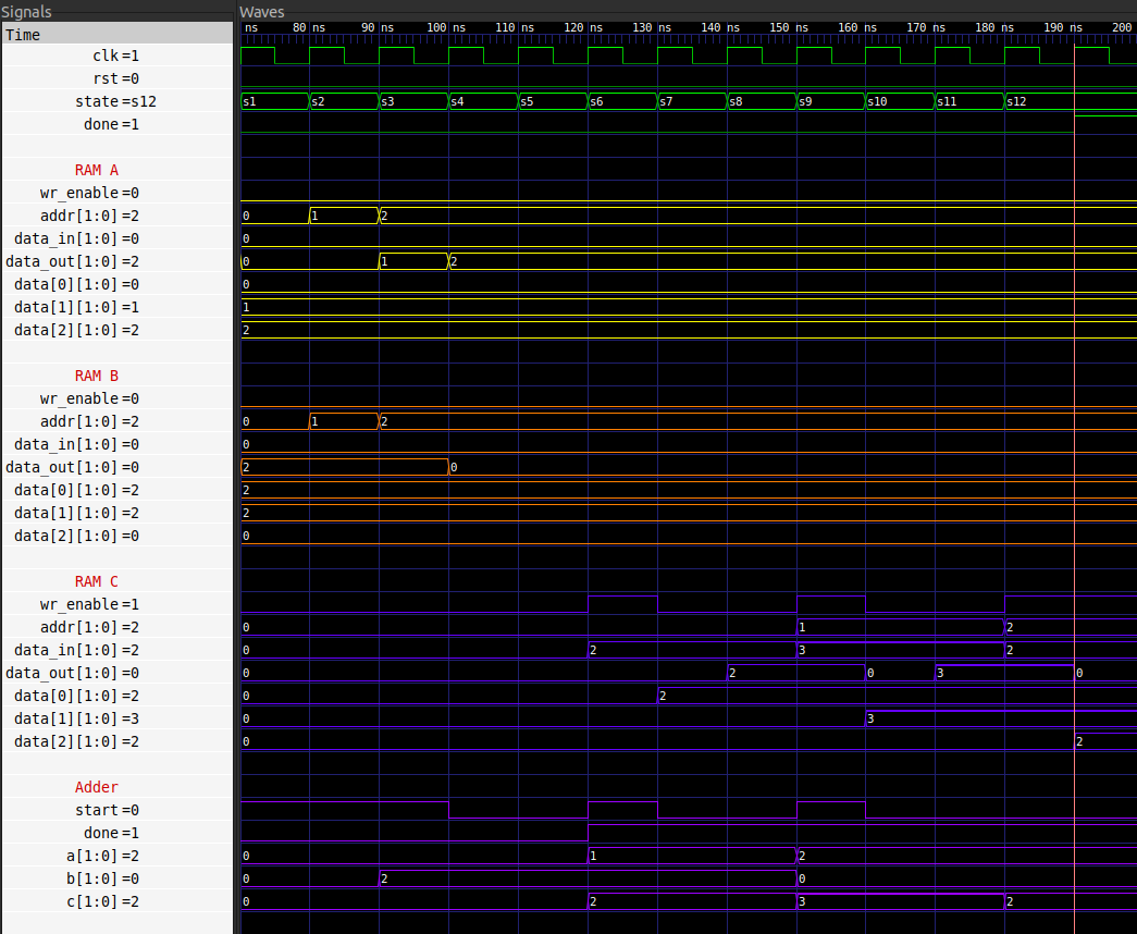
The following is the trace from the FSMD which implements the vector addition kernel as scheduled above:

Hopefully it's clear that the above matches up well with the schedule we depicted; on the first, second and third clock rising edges, RAMs A and B are presented with as ascending address, and on the following cycles the corresponding data_out ports from the RAM modules contain the values at those locations. In the adder module, the start signal is deasserted on cycles four, seven and ten indicating that the addition commences on the previous cycles (three, six and nine) in accordance with our schedule, and the result on the c port transitions on cycles six, nine and twelve; this port then directly feeds into the data_in port on RAM C, whose wr_enable is asserted the same cycle, storing the value at the provided address. The contents of RAM C are then [2, 3, 2], as expected, from cycle thirteen onwards.